
27. Md E. H. Bhuiyan, C. Wang, M. J. Arellano-Jimenez, M. Waliullah, M. Quevedo-Lopez, R. A. Bernal, M. Minary, “Electrical Property-Microstructure of Copper Interconnects Printed by Localized Pulsed Electrodeposition (L-PED)”, Materials Letters, V330, 133364 (2023).
Abstract
Printing processes that enable printing high conductivity metals at small scale (<mm) are in demand for microelectronics, interconnects, and sensors applications. Since electrical properties of metals are controlled by their microstructure, microstructure-property relation for each process needs to be established. In the recently developed localized pulsed electrodeposition (l-PED) process, the pulsed voltage applied during metal printing allows control over the microstructure. In this article, we quantify the electrical resistivity of copper (Cu) interconnects printed by the l-PED process and correlate it with its microstructure. The results show a microstructure combined of nanotwinned (nt) grains and nanocrystalline (nc) grains, with an average grain size of 190 nm and twin thickness of ∼8 nm to ∼29 nm. The electrical resistivity was measured to be 8.25 µΩ.cm, which correlates with the observed microstructure and is remarkable for a printing process with no post-processing annealing done on the printed metal.
26. B. Ojeda, M. Waliullah, A. A. Hossain, T. Nguyen, T. Wettstein, Y. Tadesse, R. A. Bernal, “High-throughput tensile testing of silver nanowires”, Extreme Mechanics Letters, V57, 101896 (2022).
Abstract
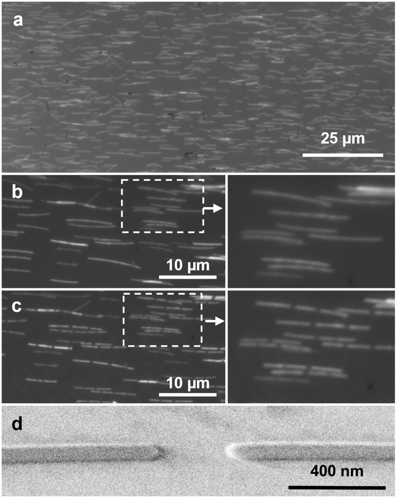
Silver nanowires (Ag NWs) have been used in various nanostructured materials such as stretchable electronics due to their small size, high strength, and high conductivity. Envisioned nanostructured materials employ millions of nanostructures to achieve its function, yet due to challenges in sample preparation, mechanical characterization has been limited to a small number of samples. The results thus have limited statistical significance, important, for example, for the case of fracture strain, which is a stochastic variable. Here, we show highly-dense and unidirectional alignment of penta-twinned Ag NWs on top of polyethylene terephthalate (PET) substrates using microfluidics. Surface treatment enabled strong bonding between NWs and substrates. We then conducted tensile stretching of the substrates in the direction of alignment, capturing images of the induced deformation and fracture of the NWs, effectively testing many of them in tension simultaneously. We analyzed their fracture strain using digital image correlation (DIC). We show results for more than 200 samples, achieving a statistical quantification of NW fracture strain, useful for the design of applications and nanostructured materials based on them, such as stretchable electronics.
25. J. H. Liang, Z. Milne, M. Rouhani, Y. Lin, R. A. Bernal, T. Sato, R. W. Carpick, Y. R. Jeng, “Stress-dependent adhesion and sliding-induced nanoscale wear of diamond-like carbon studied using in situ TEM nanoindentation”, Carbon, V193, p. 230-241 (2022).
Abstract
We present the first in situ transmission electron microscope (TEM) study of extended sliding of diamond-like carbon (DLC) on diamond. We show how the tribological properties of amorphous carbon (a-C) reach their limit by exploring the onset of wear for the harsh condition of sliding against diamond in vacuum. A particularly hard, hydrogen-free member of the DLC family, a-C is of wide technological interest, but the mechanisms by which damage occurs during tribological contact are not well understood. Real-time TEM imaging of the nanoscale contact area provides insight into wear mechanisms and damage. We show that at high normal stresses with full sliding contributing to additional shear stress, the initially low adhesion of the a-C-diamond interface rapidly increases at a rate greater than is seen in similar silicon-diamond contact studies. We propose that high contact stresses wear away a relatively low surface energy sp2-rich layer on the outer a-C surface, exposing sp3-rich sub-layers which can form covalent bonds that require more tensile force to be broken, leading to higher adhesion and an acceleration of wear.
24. G. Gleason, K. Bailey, S. Sunny, A. Malik, R. A. Bernal, “Influence of surface roughness on the transient interfacial phenomena in laser impact welding”, Journal of Manufacturing Processes, V80, p. 480-490 (2022).
Abstract
Presented is an investigation into laser impact welding (LIW) wherein experimentally measured surface profiles of the flyer and target foils are incorporated to study their effects on the transient physical phenomena that occur during this rapid, collision-based joining process. During LIW, thermal response, plastic strains, and shear stresses evolve over a sub-microsecond timescale, which necessitates the use of computational modeling to predict the influence that surface roughness has on the material response and resulting joint morphology. White light interferometry is used to experimentally characterize the surface profiles of an aluminum 1100 flyer foil and a stainless steel 304 target foil. The profiles are mapped to material volumes within a plane strain, thermomechanical simulation employing an Eulerian framework. A spatially and temporally varying laser-induced plasma pressure is applied to the flyer foil, and the resulting transient phenomena are analyzed at timeframes ranging from initial contact through complete weld formation. To reveal effects of the rough foil surfaces, results from the same computational model using smooth foil surfaces are also obtained. When the rough surface profiles are included, it is found that significant differences in the thermal response and plastic strains are observed, and these differences are hypothesized to arise from the effects of discontinuous surface contact along the collision path. The incorporation of rough surface asperities also reveals two distinct regions prior to the weld initiation point; the first where elastic rebound occurs at a negligible collision angle, leaving interfacial voids, and the second where superficial shear deformation flattens the surfaces without mutual ablation and jetting. The work represents the first study in which measured surface profiles of the flyer and target foils are incorporated into a computational model of laser impact welding.
23. M. Waliullah, R. A. Bernal, “Current density at failure of twinned silver nanowires”, Nanotechnology, V33, No. 30, 305706 (2022).
Abstract
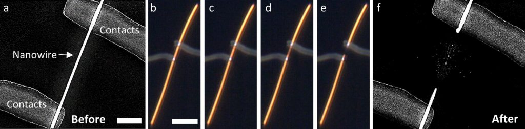
Silver nanowires have a wide range of potential applications in stretchable and transparent electronics due to their excellent electrical, mechanical, and optical properties. For a successful application in electronic devices, evaluating the electrical reliability of these nanowires is required. We have studied experimentally the behavior of current density at failure for penta-twinned silver nanowires with diameters between 53 and 173 nm, for 93 samples. The current densities at failure are widely scattered, have an average of 9.7 × 10^7 A/cm^2, and a standard deviation of 2.96 × 10^7 A/cm^2. Heat-transfer modeling is employed to explain the results, and Weibull statistics are used to quantify failure probabilities, thus offering guidelines for future designs based on these nanowires. The scatter observed in the measurements is attributed to surface-roughness variations among samples, which lead to local hot spots of high current density. These results quantify the Joule heating electrical reliability of silver nanowires and highlight the importance of heat transfer in increasing it.
22. R. A. Bernal, “On the application of Weibull statistics for describing strength of micro and nanostructures”, Mechanics of Materials, V162, 104057 (2021).
Abstract
Although the Weibull distribution has been used to describe strength data at the micro/nanoscale, its general applicability for micro/nanostructures has yet not been established. Most results are inconclusive due to insufficient data (an unavoidable challenge in micro/nanomechanical testing), and because they do not reveal the characteristics of the representative volume element. Macroscale structures are assumed to contain thousands of elements or more—the mathematical form of the Weibull distribution arises from this assumption. Micro/nanostructures, on the other hand, may contain much fewer elements. Another macroscale assumption is that the stress is far smaller than the strength of the representative element, i.e. the theoretical strength, but the strength of nanostructures approaches this value. The traditional mathematical form of the distribution also precludes calculation of the representative volume from strength data, preventing comparisons to defects or microstructural features that control failure (their size should be similar). Here, it is demonstrated that the Weibull distribution can mathematically describe the probability of failure with <5% error for a structure containing as few as 6 elements, provided the Weibull modulus > 2. Furthermore, using the exact form of the distribution, without the assumptions that lead to its traditional exponential form, equations are derived that allow the representative volume to be calculated from strength data, provided sufficient specimens and sizes are tested. Data for graphene and polysilicon are analyzed with the newly-derived equations, obtaining representative elements that agree well with the observed defects.
21. Zachary B. Milne, R. A. Bernal, Robert W. Carpick, “Sliding History-Dependent Adhesion of Nanoscale Silicon Contacts Revealed by in situ Transmission Electron Microscopy”, Langmuir, V128, p. 267-276 (2019).
Abstract
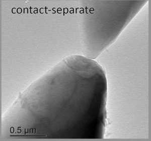
Nanoscale asperity-on-asperity sliding experiments were conducted using a nanoindentation apparatus inside a transmission electron microscope, allowing for atomic-scale resolution of contact formation, sliding, and adhesive separation of two silicon nanoasperities in real time. Forming and separating the contacts without sliding reveals adhesion forces often below detectable limits (ca. 5 nN) or at most equal to values expected from van der Waals forces. Lateral sliding during contact by distances ranging from 3.7 µm down to as little as 20 nm resulted in an average 19-times increase in the adhesive pull-off force, with increases as large as 32 times seen. Adhesion after sliding increased with both the sliding speed and the applied normal contact stress. Unlike cold welding, where irreversible material changes like flow occur, these effects were repeatable and reversible multiple times, for multiple pairs of asperities. We hypothesize that sliding removes passivating surface terminal species, most likely hydrogen or hydroxyl groups, making sites available to form strong covalent bonds across the interface that increase adhesion. Upon separation, repassivation occurs within the experimentally limited lower bound time frame of five seconds, with full recovery of low adhesion. The results demonstrate the strong sliding history-dependence of adhesion, which hinges on the interplay between tribologically-induced removal of adsorbed species and repassivation of unsaturated bonds on freshly separated surfaces by dissociative chemisorption.
20. R. A. Bernal, Robert W. Carpick, “Visualization of nanoscale wear mechanisms in ultrananocrystalline diamond by in-situ TEM tribometry”, Carbon, V54, p. 132-139 (2019).
Abstract
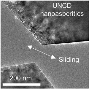
We visualize and quantify wear of ultrananocrystalline diamond (UNCD) nanoscale asperities in sliding contact using in-situ transmission electron microscope (TEM) sliding experiments. By comparing high-resolution TEM images obtained before and after a series of sliding intervals and measuring the normal force, we quantify the evolution of the specific wear rate and visualize the morphological and crystal-structure changes as wear progresses. When two sharp UNCD asperities are slid against each other, the wear rate is initially as high as ∼0.4 mm^3/N·m, but decreases substantially after a few micrometers of sliding to 10−3 – 10−2 mm^3/N·m. This latter wear rate is much larger than that observed in macroscale, multiasperity low-humidity experiments (∼10−5 mm^3/N·m). When a sharp UNCD asperity is slid against a UNCD flat, the wear rate is similarly high at the beginning, but decreases to slightly lower values, sometimes approaching ∼10−4 mm^3/N·m. In both cases, generation of amorphous debris is evident, providing in-situ confirmation of previous observations in both atomistic simulations and macroscale experiments. Gradual wear of grains and embedded crystallites in the amorphous debris are also observed. Our experiments suggest amorphization, gradual atomic-scale wear, and fracture all play a role in the nanoscale wear process of self-mated UNCD nanocontacts.
19. R. A. Bernal, Polun Chen, David Schall, Judith A.Harrison, Yeau-Ren Jeng, Robert W. Carpick, “Influence of chemical bonding on the variability of diamond-like carbon nanoscale adhesion”, Carbon, V128, p. 267-276 (2018).
Abstract
Diamond-like-carbon (DLC) is a promising material for tribological applications such as hard disk, automotive, machine tool, and aerospace coatings. We performed in-situ transmission electron microscopy (TEM) and molecular dynamics (MD) studies of nanoscale single-asperities made of tetrahedral amorphous carbon (ta-C, a type of DLC with high strength) contacting single-crystal diamond, to understand the factors controlling adhesion. Visualization of the contacts in TEM enabled us to correlate the asperity’s geometry and the adhesion measurements. MD simulations allowed the atomic-scale mechanisms of adhesion to be elucidated and correlated with the TEM observations. Experimentally-determined pull-in forces show less scatter than pull-off forces. The magnitude of the pull-in forces is consistent with adhesion arising from van der Waals (VDW) interactions, allowing us to estimate the ta-C/diamond Hamaker constant. MD simulations with the AIREBO potential confirmed that including VDW interactions leads to less scatter in adhesive forces in approach than in separation. MD simulations with the REBO+S potential demonstrate that the large scatter in pull-off forces observed experimentally arises from the complex nature of covalent bonding between substrate and tip, influenced by the local energy landscape, hydrogen coverage, and the number of repeated contact events. The scatter in pull-off force also tends to decrease with increasing roughness.
18. Soheil Daryadel, Ali Behroozfar, S. Reza Morsali, Salvador Moreno, Mahmoud Baniasadi, Julia Bykova, R. A. Bernal, Majid Minary-Jolandan, “Localized Pulsed Electrodeposition Process for Three-Dimensional Printing of Nanotwinned Metallic Nanostructures”, Nano Letters, V18, p. 208-214 (2018).
Abstract
Nanotwinned-metals (nt-metals) offer superior mechanical (high ductility and strength) and electrical (low electromigration) properties compared to their nanocrystalline (nc) counterparts. These properties are advantageous in particular for applications in nanoscale devices. However, fabrication of nt-metals has been limited to films (two-dimensional) or template-based (one-dimensional) geometries, using various chemical and physical processes. In this Letter, we demonstrate the ambient environment localized pulsed electrodeposition process for direct printing of three-dimensional (3D) freestanding nanotwinned-Copper (nt-Cu) nanostructures. 3D nt-Cu structures were additively manufactured using pulsed electrodeposition at the tip of an electrolyte-containing nozzle. Focused ion beam (FIB) and transmission electron microscopy (TEM) analysis revealed that the printed metal was fully dense, and was mostly devoid of impurities and microstructural defects. FIB and TEM images also revealed nanocrystalline-nanotwinned-microstructure (nc-nt-microstructure), and confirmed the formation of coherent twin boundaries in the 3D-printed Cu. Mechanical properties of the 3D-printed nc-nt-Cu were characterized by direct printing (FIB-less) of micropillars for in situ SEM microcompression experiments. The 3D-printed nc-nt-Cu exhibited a flow stress of over 960 MPa, among the highest ever reported, which is remarkable for a 3D-printed material. The microstructure and mechanical properties of the nc-nt-Cu were compared to those of nc-Cu printed using the same process under direct current (DC) voltage.
17. Ali Behroozfar, Soheil Daryadel, S. Reza Morsali, Salvador Moreno, Mahmoud Baniasadi, R. A. Bernal, Majid Minary-Jolandan, “Microscale 3D Printing of Nanotwinned Copper”, Advanced Materials, V30, p. 1705107 (2018).
Abstract
Nanotwinned (nt)-metals exhibit superior mechanical and electrical properties compared to their coarse-grained and nanograined counterparts. nt-metals in film and bulk forms are obtained using physical and chemical processes including pulsed electrodeposition (PED), plastic deformation, recrystallization, phase transformation, and sputter deposition. However, currently, there is no process for 3D printing (additive manufacturing) of nt-metals. Microscale 3D printing of nt-Cu is demonstrated with high density of coherent twin boundaries using a new room temperature process based on localized PED (L-PED). The 3D printed nt-Cu is fully dense, with low to none impurities, and low microstructural defects, and without obvious interface between printed layers, which overall result in good mechanical and electrical properties, without any postprocessing steps. The L-PED process enables direct 3D printing of layer-by-layer and complex 3D microscale nt-Cu structures, which may find applications for fabrication of metamaterials, sensors, plasmonics, and micro/nanoelectromechanical systems.
16. R. Ramachandramoorthy, W. Gao, R. A. Bernal, Horacio Espinosa, “High strain rate tensile testing of silver nanowires: rate-dependent brittle-to-ductile transition”, Nano Letters, V16, p 255–263 (2016).
Abstract
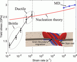
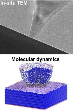
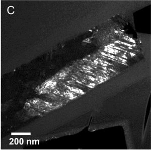
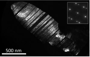
The characterization of nanomaterials under high strain rates is critical to understand their suitability for dynamic applications such as nanoresonators and nanoswitches. It is also of great theoretical importance to explore nanomechanics with dynamic and rate effects. Here, we report in situ scanning electron microscope (SEM) tensile testing of bicrystalline silver nanowires at strain rates up to 2/s, which is 2 orders of magnitude higher than previously reported in the literature. The experiments are enabled by a microelectromechanical system (MEMS) with fast response time. It was identified that the nanowire plastic deformation has a small activation volume (<10b3), suggesting dislocation nucleation as the rate controlling mechanism. Also, a remarkable brittle-to-ductile failure mode transition was observed at a threshold strain rate of 0.2/s. Transmission electron microscopy (TEM) revealed that along the nanowire, dislocation density and spatial distribution of plastic regions increase with increasing strain rate. Furthermore, molecular dynamic (MD) simulations show that deformation mechanisms such as grain boundary migration and dislocation interactions are responsible for such ductility. Finally, the MD and experimental results were interpreted using dislocation nucleation theory. The predicted yield stress values are in agreement with the experimental results for strain rates above 0.2/s when ductility is pronounced. At low strain rates, random imperfections on the nanowire surface trigger localized plasticity, leading to a brittle-like failure.
15. R. A. Bernal, A. Aghaei, S. Lee, S. Ryu, K. Sohn, J. Huang, W. Cai, H. D. Espinosa, “Intrinsic Bauschinger Effect and Recoverable Plasticity in Penta-twinned Silver Nanowires Tested in Tension”, Nano Letters, V15, p. 139-146 (2015).
Abstract
Silver nanowires are promising components of flexible electronics such as interconnects and touch displays. Despite the expected cyclic loading in these applications, characterization of the cyclic mechanical behavior of chemically synthesized high-quality nanowires has not been reported. Here, we combine in situ TEM tensile tests and atomistic simulations to characterize the cyclic stress–strain behavior and plasticity mechanisms of pentatwinned silver nanowires with diameters thinner than 120 nm. The experimental measurements were enabled by a novel system allowing displacement-controlled tensile testing of nanowires, which also affords higher resolution for capturing stress–strain curves. We observe the Bauschinger effect, that is, asymmetric plastic flow, and partial recovery of the plastic deformation upon unloading. TEM observations and atomistic simulations reveal that these processes occur due to the pentatwinned structure and emerge from reversible dislocation activity. While the incipient plastic mechanism through the nucleation of stacking fault decahedrons (SFDs) is fully reversible, plasticity becomes only partially reversible as intersecting SFDs lead to dislocation reactions and entanglements. The observed plastic recovery is expected to have implications to the fatigue life and the application of silver nanowires to flexible electronics.
14. R. Ramachandramoorthy, R. A. Bernal and H.D. Espinosa, “Pushing the Envelope of In Situ Transmission Electron Microscopy”, ACS Nano, V9, p. 4675–4685 (2015).
Abstract
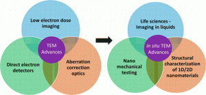
Recent major improvements to the transmission electron microscope (TEM) including aberration-corrected electron optics, light-element-sensitive analytical instrumentation, sample environmental control, and high-speed and sensitive direct electron detectors are becoming more widely available. When these advances are combined with in situ TEM tools, such as multimodal testing based on microelectromechanical systems, key measurements and insights on nanoscale material phenomena become possible. In particular, these advances enable metrology that allows for unprecedented correlation to quantum mechanics and the predictions of atomistic models. In this Perspective, we provide a summary of recent in situ TEM research that has leveraged these new TEM capabilities as well as an outlook of the opportunities that exist in the different areas of in situ TEM experimentation. Although these advances have improved the spatial and temporal resolution of TEM, a critical analysis of the various in situ TEM fields reveals that further progress is needed to achieve the full potential of the technology.
13. R. A. Bernal, R. Ramachandramoorthy and H.D. Espinosa, “Double-tilt in situ TEM holder with multiple electrical contacts and its application in MEMS-based mechanical testing of nanomaterials”, Ultramicroscopy, V156, p. 23-28 (2015).
Abstract
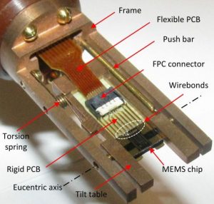
MEMS and other lab-on-a-chip systems are emerging as attractive alternatives to carry out experiments in situ the electron microscope. However, several electrical connections are usually required for operating these setups. Such connectivity is challenging inside the limited space of the TEM side-entry holder. Here, we design, implement and demonstrate a double-tilt TEM holder with capabilities for up to 9 electrical connections, operating in a high-resolution TEM. We describe the operating principle of the tilting and connection mechanisms and the physical implementation of the holder. To demonstrate the holder capabilities, we calibrate the tilting action, which has limits of ±15°, and establish the insulation resistance of the electronics to be 36 GΩ, appropriate for measurements of currents down to the nano-amp (nA) regime. Furthermore, we demonstrate tensile testing of silver nanowires using a previously developed MEMS device for mechanical testing, using the implemented holder as the platform for electronic operation and sensing. The implemented holder can potentially have broad application to other areas where MEMS or electrically-actuated setups are used to carry out in situ TEM experiments.
12. M.F. Pantano, R.A. Bernal, L. Pagnotta and H.D. Espinosa, “Multiphysics design and implementation of a microsystem for displacement-controlled tensile testing of nanomaterials”, Meccanica, V50, p. 549-560 (2015).
Abstract
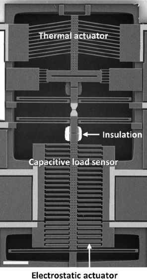
MEMS-based tensile testing devices are powerful tools for mechanical characterization of nanoscale materials. In a typical configuration, their design includes an actuator to deliver loads/displacements to a sample, and a sensing unit for load measurement. The sensing unit consists of a flexible structure, which deforms in response to the force imposed to the sample. Such deformation, while being necessary for the sensing function, may become a source of instability. When the sample experiences a load drop, as it may result from yield, necking or phase transitions, the elastic energy accumulated by the sensor can be released, thus leading to loss of the displacement-controlled condition and dynamic failure. Here, we report a newly-developed MEMS testing system where the sensor is designed to constantly keep its equilibrium position through an electrostatic feedback-control. We show design, implementation, and calibration of the system, as well as validation by tensile testing of silver nanowires. The implemented system allows capture of softening events and affords significant improvement on the resolution of stress–strain curves.
11. R. A. Bernal, T. Filleter, J. G. Connell, K. Sohn, J. Huang, L. J. Lauhon, and H. D. Espinosa, “In Situ Electron Microscopy Four-Point Electromechanical Characterization of Freestanding Metallic and Semiconducting Nanowires”, Small, V10, p. 725–733 (2014)
Abstract
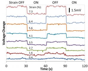
Electromechanical coupling is a topic of current interest in nanostructures, such as metallic and semiconducting nanowires, for a variety of electronic and energy applications. As a result, the determination of structure-property relations that dictate the electromechanical coupling requires the development of experimental tools to perform accurate metrology. Here, a novel micro-electro-mechanical system (MEMS) that allows integrated four-point, uniaxial, electromechanical measurements of freestanding nanostructures in-situ electron microscopy, is reported. Coupled mechanical and electrical measurements are carried out for penta-twinned silver nanowires, their resistance is identified as a function of strain, and it is shown that resistance variations are the result of nanowire dimensional changes. Furthermore, in situ SEM piezoresistive measurements on n-type, [111]-oriented silicon nanowires up to unprecedented levels of ∼7% strain are demonstrated. The piezoresistance coefficients are found to be similar to bulk values. For both metallic and semiconducting nanowires, variations of the contact resistance as strain is applied are observed. These variations must be considered in the interpretation of future two-point electromechanical measurements.
10. H.D. Espinosa, R. A. Bernal and M.M. Jolandan, “A Review of Mechanical and Electromechanical Properties of Piezoelectric Nanowires”, Advanced Materials, V24, p. 4656–4675 (2012).
Abstract
Piezoelectric nanowires are promising building blocks in nanoelectronic, sensing, actuation and nanogenerator systems. In spite of great progress in synthesis methods, quantitative mechanical and electromechanical characterization of these nanostructures is still limited. In this article, the state-of-the art in experimental and computational studies of mechanical and electromechanical properties of piezoelectric nanowires is reviewed with an emphasis on size effects. The review covers existing characterization and analysis methods and summarizes data reported in the literature. It also provides an assessment of research needs and opportunities. Throughout the discussion, the importance of coupling experimental and computational studies is highlighted. This is crucial for obtaining unambiguous size effects of nanowire properties, which truly reflect the effect of scaling rather than a particular synthesis route. We show that such a combined approach is critical to establish synthesis-structure-property relations that will pave the way for optimal usage of piezoelectric nanowires.
9. J.R. Riley, R. A. Bernal, Q. Li, H.D. Espinosa, G.T. Wang and L.J. Lauhon, “Atom Probe Tomography of a-Axis GaN Nanowires: Analysis of Nonstoichiometric Evaporation Behavior”, ACS Nano, V6, p. 3898–3906 (2012).
Abstract
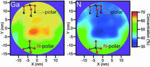
GaN nanowires oriented along the nonpolar a-axis were analyzed using pulsed laser atom probe tomography (APT). Stoichiometric mass spectra were achieved by optimizing the temperature, applied dc voltage, and laser pulse energy. Local variations in the measured stoichiometry were observed and correlated with facet polarity using scanning electron microscopy. Fewer N atoms were detected from nonpolar and Ga-polar surfaces due to uncorrelated evaporation of N2 ions following N adatom diffusion. The observed differences in Ga and N ion evaporation behaviors are considered in detail to understand the influence of intrinsic materials characteristics on the reliability of atom probe tomography analysis. We find that while reliable analysis of III–N alloys is possible, the standard APT procedure of empirically adjusting analysis conditions to obtain stoichiometric detection of Ga and N is not necessarily the best approach for this materials system.
8. H.D. Espinosa, R. A. Bernal and T. Filleter, “In Situ TEM Electromechanical Testing of Nanowires and Nanotubes”, Small, V8, p. 3233-3252 (2012). Also appears as a book chapter in Nano and Cell Mechanics: Fundamentals and Frontiers, Wiley. 2013.
Abstract

The emergence of one-dimensional nanostructures as fundamental constituents of advanced materials and next-generation electronic and electromechanical devices has increased the need for their atomic-scale characterization. Given its spatial and temporal resolution, coupled with analytical capabilities, transmission electron microscopy (TEM) has been the technique of choice in performing atomic structure and defect characterization. A number of approaches have been recently developed to combine these capabilities with in-situ mechanical deformation and electrical characterization in the emerging field of in-situ TEM electromechanical testing. This has enabled researchers to establish unambiguous synthesis-structure-property relations for one-dimensional nanostructures. In this article, the development and latest advances of several in-situ TEM techniques to carry out mechanical and electromechanical testing of nanowires and nanotubes are reviewed. Through discussion of specific examples, it is shown how the merging of several microsystems and TEM has led to significant insights into the behavior of nanowires and nanotubes, underscoring the significant role in-situ techniques play in the development of novel nanoscale systems and materials.
7. T. Filleter, R. Seunghwa, J. Yin, K. Kang, R. A. Bernal, K. Sohn, S. Li, J. Huang, W. Cai, and H. D. Espinosa, “Nucleation-controlled distributed plasticity in penta-twinned silver nanowires”, Small, V8, p. 2986–2993 (2012).
Abstract
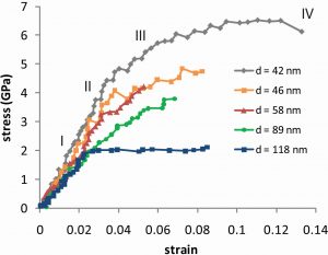
A unique size-dependent strain hardening mechanism, that achieves both high strength and ductility, is demonstrated for penta-twinned Ag nanowires (NWs) through a combined experimental-computational approach. Thin Ag NWs are found to deform via the surface nucleation of stacking fault decahedrons (SFDs) in multiple plastic zones distributed along the NW. Twin boundaries lead to the formation of SFD chains that locally harden the NW and promote subsequent nucleation of SFDs at other locations. Due to surface undulations, chain reactions of SFD arrays are activated at stress concentrations and terminated as local stress decreases, revealing insensitivity to defects imparted by the twin structures. Thick NWs exhibit lower flow stress and number of distributed plastic zones due to the onset of necking accompanied by more complex dislocation structures.
6. R. A. Bernal, R. Agrawal, B. Peng, K.A. Bertness, N.A. Sanford, A.V. Davydov and H.D. Espinosa, “Effect of Growth Orientation and Diameter on the Elasticity of GaN Nanowires. A Combined in Situ TEM and Atomistic Modeling Investigation”, Nano Letters, V11, p. 548–555 (2011).
Abstract
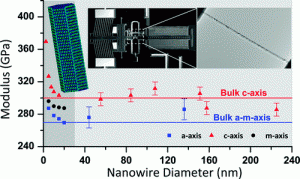
We characterized the elastic properties of GaN nanowires grown along different crystallographic orientations. In situ transmission electron microscopy tensile tests were conducted using a MEMS-based nanoscale testing system. Complementary atomistic simulations were performed using density functional theory and molecular dynamics. Our work establishes that elasticity size dependence is limited to nanowires with diameters smaller than 20 nm. For larger diameters, the elastic modulus converges to the bulk values of 300 GPa for c-axis and 267 GPa for a– and m-axis.
5. M.M.-Jolandan, R. A. Bernal, I. Kuljanishvili, V. Parpoil, and H.D. Espinosa, “Individual GaN Nanowires Exhibit Strong Piezoelectricity in 3D”, Nano Letters, V12, p. 970-976 (2011).
Abstract
Semiconductor GaN NWs are promising components in next generation nano- and optoelectronic systems. In addition to their direct band gap, they exhibit piezoelectricity, which renders them particularly attractive in energy harvesting applications for self-powered devices. Nanowires are often considered as one-dimensional nanostructures; however, the electromechanical coupling leads to a third rank tensor that for wurtzite crystals (GaN NWs) possesses three independent coefficients, d33, d13, and d15. Therefore, the full piezoelectric characterization of individual GaN NWs requires application of electric fields in different directions and measurements of associated displacements on the order of several picometers. In this Letter, we present an experimental approach based on scanning probe microscopy to directly quantify the three-dimensional piezoelectric response of individual GaN NWs. Experimental results reveal that GaN NWs exhibit strong piezoelectricity in three dimensions, with up to six times the effect in bulk. Based on finite element modeling, this finding has major implication on the design of energy harvesting systems exhibiting unprecedented levels of power density production. The presented method is applicable to other piezoelectric NW materials as well as wires manufactured along different crystallographic orientations.
4. M.M.-Jolandan, R. A. Bernal and H.D. Espinosa, “Strong piezoelectricity in individual GaN nanowires”, MRS Communications, V1, p. 45-48 (2011).
Abstract
GaN nanowires are promising building blocks for future nanoelectronics, optoelectronic devices, and nanogenerators. Here, we report on strong piezoelectricity in individual single-crystal GaN nanowires revealed by direct measurement of the piezoelectric constant using piezoresponse force microscopy. Our experimental results show that individual c-axis GaN nanowires, with a characteristic dimension as small as 65 nm, show a shear piezoelectric constant of d15 ~ 10 pm/V, which is several times that measured in bulk. The revealed strong piezoelectricity could open promising opportunities for application of GaN nanowires in nanowire-based sensors and generators for self-powered nanodevices.
3. R. Agrawal, R. A. Bernal, D. Isheim, H.D. Espinosa, “Characterizing Atomic Composition and Dopant Distribution in Wide Band Gap Semiconductor Nanowires Using Laser-Assisted Atom Probe Tomography”, The Journal of Physical Chemistry C, V115, p. 17688–17694 (2011).
Abstract
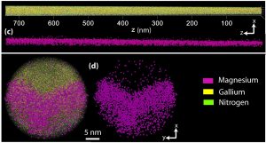
Characterization of atomic composition and spatially resolved dopant distribution in wide band gap semiconducting nanowires is critical for their applications in next-generation nanoelectronic and optoelectronic devices. We have applied laser-assisted atom probe tomography to measure the spatially resolved composition of wide band gap semiconducting undoped GaN nanowires and Mg-doped GaN nanowires. Stoichiometric evaporation of individual GaN nanowires was achieved, and optimal experimental conditions to characterize the concentration and spatial distribution of the dopant in the Mg:GaN nanowire samples were established. Extremely mild operating conditions, with laser pulse energy as low as 3 pJ, are required to avoid preferential loss of nitrogen and achieve stoichiometric evaporation. The role of nanowire morphology in the selection of optimal experimental conditions is discussed in the context of thermal transport within the nanowire under a heat load imposed by the pulsing laser. The results of this work are expected to help guide similar atom probe tomography studies of related wide band gap III–V semiconductor alloys, which will facilitate a better understanding of material response and will help develop structure–property relationships.
2. T. Filleter, R. A. Bernal, S. Li, and H.D. Espinosa, “Ultrahigh Strength and Stiffness in Cross-Linked Hierarchical Carbon Nanotube Bundles”, Advanced Materials, Vol. 23, No. 25, p. 2855-2860, (2011).
Abstract
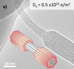
Electron-irradiation-induced, covalent, cross-linking at multiple length scales within double-walled nanotube bundles is demonstrated to lead to ultrahigh effective strength and stiffness. In situ transmission electron microscopy tensile testing reveals both order of magnitude enhancements in the mechanical properties as well as distinct failure mechanisms of cross-linked versus un-crosslinked bundles.
1. R. A. Bernal, A. Avila, “Reproducible Fabrication of Scanning Tunneling Microscope Tips”, Revista de Ingeniería, n27, p. 43-48, (2008).
Abstract
Reproducible fabrication of Scanning Tunneling Microscope tips is carried out following an electrochemical procedure widely reported. Tips are made from 0.5 mm diameter tungsten wire. Controlling fabrication parameters (immersion in the electrochemical solution, current-voltage ranges, duration of the process, among others) we achieve aspect ratios of 0.68 and tip radii of 330 nm in the best case.