Nanomechanical Multiphysics
Our vision is to aid in the development of next-generation sensing and electronic devices by discovering and understanding novel nanomechanical multiphysics phenomena, where mechanical deformation can tune and control other physical domains (electrical, thermal, chemical). Our research is important in the context of the current state of the electronics industry, because increased progress in sensing and electronics do not depend anymore on just more miniaturization, since the fundamental scaling limits of transistors will be reached in the near future.
Instead, future electronics will have to be complemented by integration of multiple innovative functions and sensors. This is called the More-than-Moore approach, critical for technologies such as the Internet of Things. This approach uses synergies between multiple physical domains, mechanics being prominent among them. Just to give two examples: 1. Smartphone accelerometers integrate mechanics and electronics. 2. Transistor performance has been improved by straining (stretching or compressing) silicon, thus increasing the speed at which electrons travel through it. These multiphysics synergies will deepen in the future: We can envision wearable devices, powered by our movement, gathering biochemical signals through our skin, communicating wirelessly with our doctor.
Future sensors will also be different from traditional sensors, in which sensing, transduction, signal conditioning, and data recording are separate. For example, a mechanical strain gage uses a piezoresistive metal wire, but requires a separate power supply, Wheatstone bridge electronics, and data acquisition system. A future nanosensor might operate as a strain-gated transistor, integrating sensing, transduction and signal conditioning in a single element, allowing simpler system architecture, lower energy consumption, and cost savings. This research will lead to unique opportunities to study new phenomena for novel devices with higher energy efficiency, lower costs, and better user experience.
Here is a summary of one of our research projects, as part of a 3-Minute-Thesis competition:
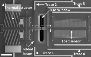
Our research program is primarily experimental, using in-situ microscopy studies as one of our main tools, and highly interdisciplinary, using concepts and techniques from Mechanics, Materials Science and Electrical Engineering. We also employ the full array of nanotechnology tools, including scanning probe microscopy and microfabrication. Please see our publications for even more details.